| Press ReleaseMay 16, 2014Tokyo Institute of Technology (Tokyo Tech) Ibaraki UniversityAustralian Nuclear Science and Technology Organization (ANSTO) Japan Synchrotron Radiation Research Institute (JASRI) SPring-8High Energy Accelerator Research Organization (KEK) Japan Proton Accelerator Research Complex (J-PARC) |
| Discovery of a New Crystal Structure Family of Oxide-Ion Conductors NdBaInO4 |
| Structure Determination and Ion Diffusion Visualization by Neutron and Synchrotron X-ray DiffractionToward Development of Fuel Cells, Sensors, and Electronic Materials |
| |
| Abstract A team led by Prof. Masatomo Yashima and Assistant Prof. Kotaro Fujii of Department of Chemistry and Materials Science of Graduate School of Science and Engineering of Tokyo Institute of Technology (Japan) , Prof. Toru Ishigaki and Associate Prof. Akinori Hoshikawa of Ibaraki University (Japan) and Dr. James R. Hester of the Australian Nuclear Science and Technology Organisation (Australia) has discovered a new structure family of oxide-ion (O2-) conducting materials 1 ) NdBaInO4 (neodium barium indium oxide) . 2 ) The team successfully determined its crystal structure 3 ) and visualized its oxide-ion diffusion pathway (Fig. 1) . The discovery of this new structure family NdBaInO4 can lead to the developments of new ionic conductors for better solid oxide fuel cells and oxygen concentrators, and of electronic materials.
The structure was analyzed using the neutron diffraction 4 ) data measured with both diffractometers (1) belonging to Ibaraki prefecture, installed at J-PARC, and (2) belonging to ANSTO, and using synchrotron X-ray diffraction 5 ) data measured at (3) SPring-8 and (4) the High Energy Accelerator Research Organization (KEK) Photon Factory. |
| |
 * Click here to enlarge. * Click here to enlarge. |
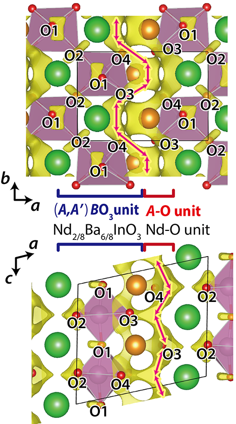
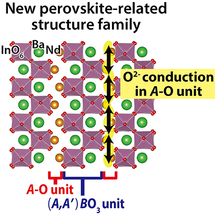
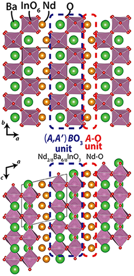
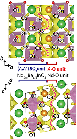
| Figure 1 : Refined crystal structure and oxide-ion diffusion pathway of NdBaInO4, which consists of (i) A-O (Nd-O) unit and (ii) (A,A') BO3 (= Nd2/8Ba6/8InO3) perovskite unit. 6 ) The oxide-ion (O2-) conduction occurs in the A-O unit (Arrows in the figure) . |
| |
| Background of this work Oxide-ion conducting materials 1 ) such as pure oxide-ion conductors and mixed oxide ion-electronic conductors have a wide variety of applications in fuel cells, oxygen separation membranes and gas sensors. Since the oxide-ion conductivity is strongly dependent on the crystal structure, the discovery of new oxide-ion conductor belonging to a new structure family may open a new window for further innovative developments in the applications of oxide-ion conductors. |
| Results of this work (1) : Discovery of new structure family of oxide-ion conducting materials NdBaInO4 To design a new layered perovskite-related structure, 6 ) the research group lead by Professor Yashima has examined various chemical compositions of AA'BO4 where A and A' are larger cations and B is smaller cation. After examining a number of chemical compositions, Professor Yashima's group discovered a new structure family of oxide-ion conducting materials NdBaInO4.
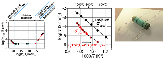
The Nd, Ba and In were chosen as cations, because (i) the different sizes of Nd and Ba can lead to the Ba/Nd cation ordering and (ii) the BaInO3 perovskite unit can form from the view point of the sizes of Ba and In cations. NdBaInO4 was prepared by solid-state reactions 7 ) at 1400 ℃ using BaCO3, In2O3 and Nd2O3 powders. NdBaInO4 exhibits oxide-ion conduction as shown in Figure 2. The present NdBaInO4 sample is a single monoclinic phase with a new crystal structure as described below. Thus a new structure family of oxide-ion conducting material NdBaInO4 was discovered in this study. |
| |
  * Click here to enlarge. * Click here to enlarge. |
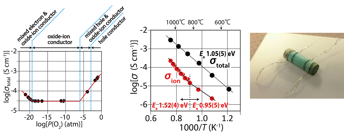
| Figure 2 : Oxygen partial pressure dependence of total electrical conductivity of NdBaInO4 (left) . Arrhenius plots 8 ) of total electrical conductivity in air and oxide-ion conductivity of NdBaInO4 (center) . NdBaInO4 sample with the Pt wires for dc electrical conductivity measurements (right) . |
| |
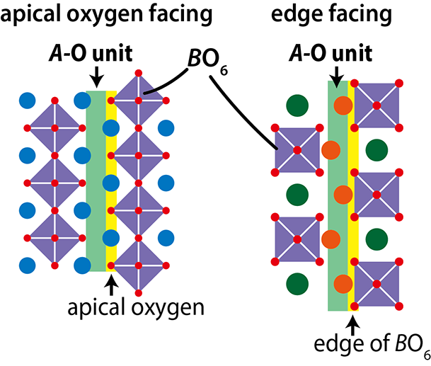
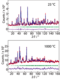
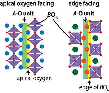
| Results of this work (2) : Crystal structure and oxygen diffusion path of NdBaInO4 Crystal structure of NdBaInO4 was investigated by neutron and synchrotron X-ray powder diffractometry (Photos 1 and 2, Figs. 3 and 4) and ab initio electronic calculations. 9 ) The research group carried out the ab initio crystal structure analysis 10 ) using the X-ray powder diffraction data. Neutron diffraction enables the precise determination of positional parameters of oxygen atoms. The space group was found to be monoclinic P21/c. 11 ) The validity of the crystal structure of NdBaInO4 (Fig. 5) was confirmed by Rietveld refinements 12 ) of synchrotron X-ray powder diffraction data measured at (i) SPring-8 and at (ii) PF, by Rietveld analysis 12 ) of neutron diffraction data measured at (iii) J-PARC and at (iv) ANSTO, (v) by bond valence sums (BVS) 13 ) of Nd, Ba and In atoms, (vi) by the structural optimization based on the density functional theory calculations. The refined crystal structure of NdBaInO4 consists of A-rare earth oxide A-O (Nd-O) and perovskite (A,A') BO3 (Nd2/8Ba6/8InO3) units (Fig. 5) , which indicates a new A/A' cation ordered perovskite-related layered structure. An outstanding and unique feature of this new structure is that the edge of the InO6 octahedron faces the A-O (Nd-O) unit (Fig. 6) . The oxide-ion diffusion path of NdBaInO4 was visualized using the bond valence method 13 ) (Fig. 7) . The oxide ions can diffuse two-dimensionally in the A-O (Nd-O) unit. |
  * Click here to enlarge. * Click here to enlarge. |
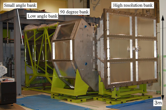
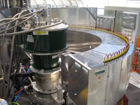
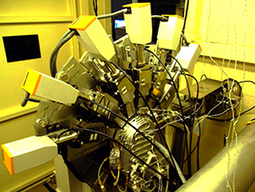
| Photo 1 : Photos of neutron diffractometers iMATERIA (left) in J-PARC and Echidna (right) of ANSTO. |
  * Click here to enlarge. * Click here to enlarge. |
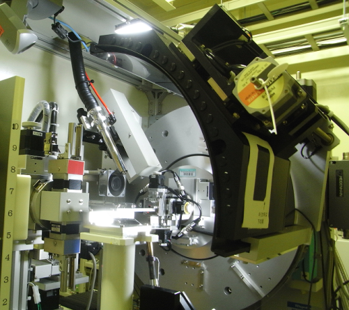
| Photo 2 : Photos of synchrotron X-ray diffractometers installed at BL19B2 of SPring-8 (left) and at BL-4B2 of PF@KEK (right) . |
| |
 * Click here to enlarge. * Click here to enlarge. |
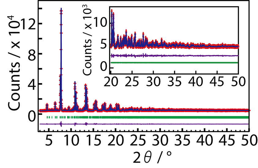
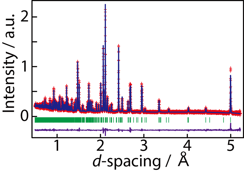
| Figure 3 : Rietveld pattern of synchrotron X-ray powder diffraction data of NdBaInO4 (27 ℃) . |
| |
  * Click here to enlarge.* Click here to enlarge. * Click here to enlarge.* Click here to enlarge. |
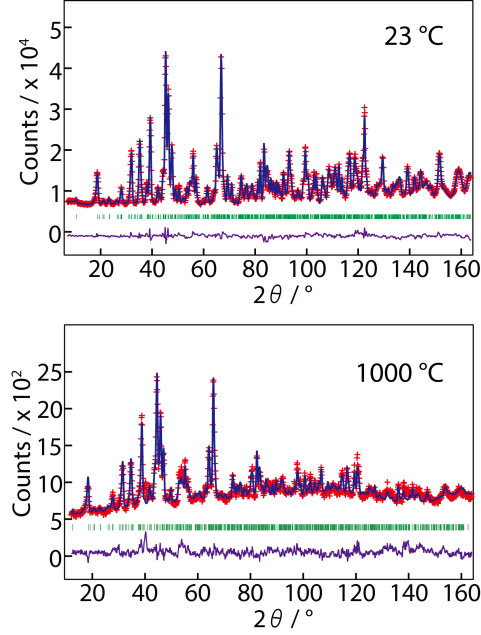
| Figure 4 : Rietveld patterns of neutron powder diffraction data of NdBaInO4 (Left: 24 ℃, iMATERIA@J-PARC; Right: 23 ℃ and 1000 ℃, Echidna@ANSTO) . |
| |
 * Click here to enlarge. * Click here to enlarge. |
| Figure 5 : Crystal structure of NdBaInO4 (24 ℃) determined in this work. |
| |
 * Click here to enlarge. * Click here to enlarge. |
| Figure 6 : Feature that the apical oxygen faces the A-O unit in conventional perovskite-related structure (left, example: K2NiF4-type oxides) . Unique feature that the edge faces the A-O unit in the new structure family (right, NdBaInO4) . |
| |
 * Click here to enlarge. * Click here to enlarge. |
| Figure 7 : Diffusion pathway of oxide ions in NdBaInO4 at 1000 ℃ (Arrows in the figure) . |
| |
| Explanation of technical terms |
| 1 ) Oxide ion conducting materials : Materials where the oxide ions can conduct when the external electric field is applied. The oxide ion conducting materials can be classified into (i) pure oxide-ion conductors and (ii) mixed oxide ion-electronic conductors. |
| 2 ) NdBaInO4 : An oxide consisting of Nd, Ba and In cations and oxide ions. |
| 3 ) Crystal structure : Crystal is the material where the atomic arrangement has exact periodicity. Crystal structure is the atomic arrangement of a crystal. The crystal structure is specified by space group (symmetry of the atomic arrangement) , unit-cell parameters (size and shape of the unit cell) , atomic coordinates (positions of atoms in the unit cell) and so on. |
| 4 ) Neutron diffraction : When free neutrons are scattered by a crystal (strictly speaking, scattered by the nuclei and spins in a crystal) , the neutrons behave like waves and are diffracted by the crystal. This phenomenon is called as neutron diffraction. Neutron diffraction enables the determination of crystal structure. Neutron diffraction can determine accurately the atomic positions of light element as oxygen in a compound consisting of light and heavy elements, compared with the X-ray diffraction. In this work we used the iMATERIA diffractometer of Ibaraki Prefecture installed in the J-PARC of Japan Atomic Energy Agency (JAEA) /KEK (Head of the Beamline Scientist : Prof. Toru Ishigaki of Ibaraki University) . We also used the Echidna diffractometer installed in ANSTO, Australia (Beamline Scientists: Dr. M. Avdeev and Dr. J. Hester) . |
| 5 ) Synchrotron X-ray diffraction : Synchrotron is an extremely bright source of X rays. When synchrotron X rays are scattered by a crystal (strictly speaking, by the electrons in a crystal) , the synchrotron X rays behave like waves and are diffracted by the crystal. This phenomenon is called as synchrotron X-ray diffraction. Synchrotron X-ray diffraction enables the determination of crystal structure. In this work, we used the powder diffractometer installed at the beamline BL-19B2 of SPring-8 with the help of Dr. K. Osaka of Japan Synchrotron Research Institute : JASRI) . We also used the multi-detector system installed at the beamline BL-4B2 of Photon Factory of KEK (Beamline Scientists: Associate Professor H. Nakao of PF, Prof. T. Ida of Nagoya Institute of Technology) . |
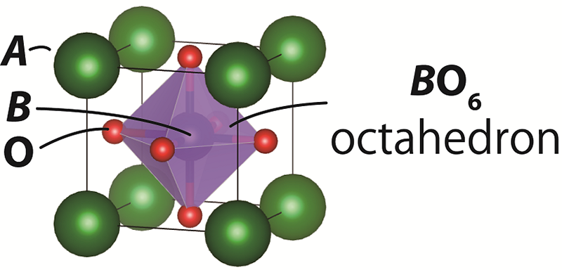
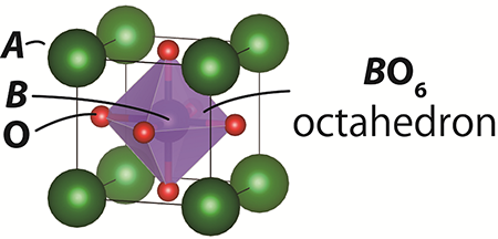
| 6 ) Perovskite-related structure; Perovskite-type structure; Perovskite unit : In the ideal cubic ABO3 perovskite-type structure, for example, the larger A cation is located at the corner of cubic unit cell, smaller B cation exists at the center of the cell, and oxygen anions are located at the face centers of the cell (Fig. 8) . The perovskite-type structure can be distorted depending on the chemical composition (combination of A and B cations and oxygen content) , temperature, pressure and oxygen partial pressure: The constituent atoms can be shifted from the ideal positions. In a crystal structure, if the atomic arrangement of a part of the crystal structure is regarded as that of an ideal or distorted ABO3 perovskite-type structure, the part is called as perovskite unit. The crystal structure containing the perovskite unit is called as the perovskite-related structure. |
 * Click here to enlarge. * Click here to enlarge. |
| Figure 8 : Ideal cubic ABO3 perovskite-type structure. |
| 7 ) Solid-state reactions : Reactions between two solid phases or among three or more solid phases. |
| 8 ) Arrhenius plot : Plot of a physical quantity such as ionic conductivity against the absolute temperature inverse. In a limited temperature range, the Arrhenius plot of ionic conductivity exhibits a linear line. From the slope of the line, we can estimate the activation energy which is the energy barrier when an ion migrates. |
| 9 ) Ab initio electronic calculations : To calculate the electronic states in a material on the basis of the quantum mechanics/chemistry without empirical parameters. In this work we optimized the crystal structure of NdBaInO4 by the ab initio electronic calculations based on the density functional theory. |
| 10 ) Ab initio crystal structure analysis : Ab initio crystal structure analysis based on the powder diffraction data is to analyze and solve the crystal structure from the powder diffraction data without initial structural model from related compounds. Usually indexing is needed in the first step. |
| 11 ) Space group P21/c : Three-dimensional crystals are classified into 230 space groups depending on their symmetries. The P21/c is the 14th space group of the 230 ones. |
| 12 ) Rietveld refinement. Rietveld analysis : From powder diffraction data, to refine the crystal structure: Using the initial structural model, the crystallographic parameters such as unit-cell and positional parameters are changed (refined) so that the agreement between the observed and calculated intensities is improved. |
| 13 ) Bond valence sum (BVS) ; Bond valence method (BVM) : BVS is calculated from interatomic distances and empirical bond valence parameters. BVM based on BVS is a method to estimate the oxidation number. The crystal structure can be validated if the BVSs agree with the oxidation numbers. The diffusion pathway can be investigated by BVM through BVS map (the spatial distribution map of BVS) in the unit cell. |
| |
|
Publication of this work |
: |
Chemistry of Materials (American Chemical Society) as Communications, 2014, 26 (8) , pp 2488-2491 |
|
|
Publication Date (Web) |
: |
March 21, 2014DOI |
|
|
Title |
: |
New perovskite-related structure family of oxide-ion conducting materials NdBaInO4 |
|
|
Authors |
: |
Kotaro Fujii (Assistant Professor, Tokyo Institute of Technology) , Yuichi Esaki (Master course student, Tokyo Institute of Technology) , Kazuki Omoto (Doctor course student, Tokyo Institute of Technology) , Masatomo Yashima* (Professor, Tokyo Institute of Technology) , Akinori Hoshikawa (Associate Professor, Ibaraki University) , Toru Ishigaki (Professor, Ibaraki University) , and James R. Hester (Dr., Instrument Scientist, ANSTO) |
|
| Prof. Masatomo YashimaDepartment of Chemistry and Materials Science, Graduate School of Science and Engineering, Tokyo Institute of Technology |
| 2-12-1-W4-17, O-okayama, Meguro-ku, Tokyo 152-8551, JapanE-mail : yashima@cms.titech.ac.jpTEL : +81-3-5734-2225FAX : +81-3-5734-2225 |
| Assistant Prof. Kotaro FujiiDepartment of Chemistry and Materials Science, Graduate School of Science and Engineering, Tokyo Institute of Technology |
| 2-12-1-W4-17, O-okayama, Meguro-ku, Tokyo 152-8551, JapanE-mail : kfujii@cms.titech.ac.jpTEL : +81-3-5734-2331FAX : +81-3-5734-2331 |
| Prof. Toru IshigakiFrontier Research Center for Applied Atomic Sciences, Ibaraki University |
| Shirakata 162-1, Tokai, Naka-gun, Ibaraki 319-1106, JapanE-mail : to_ishig@mx.ibaraki.ac.jpTEL : +81-29-352-3231FAX : +81-29-287-7872 |
| Associate Prof. Akinori Hoshikawa (Neutron Diffractiometer iMATERIA) Frontier Research Center for Applied Atomic Sciences, Ibaraki University |
| Shirakata 162-1, Tokai, Naka-gun, Ibaraki 319-1106, JapanE-mail : hoshi@mx.ibaraki.ac.jpTEL : +81-29-352-3232FAX : +81-29-287-7872 |
| Dr. James R. HesterThe Bragg Institute, Australian Nuclear Science and Technology Organisation |
| Lucas Heights, NSW 2234, AustraliaE-mail : jxh@ansto.gov.auTEL : +61-2-9717-9907FAX : +61-2-9717-3145 |
| Japan Synchrotron Radiation Research Institute (JASRI) SPring-8 |
| 1-1-1, Kouto, Sayo-cho, Sayo-gun, Hyogo 679-5198 JapanE-mail : kouhou@spring8.or.jpTEL : +81-791-58-2785FAX : +81-791-58-2786 |
| Saeko OkadaSenior Press Officer, Public Relations Office, KEK Public RelationsOffice, High Energy Accelerator Research Organization (KEK) |
| 1-1 Oho, Tsukuba, Ibaraki 305-0801 JapanE-mail : press@kek.jp TEL : +81-29-879-6046FAX : +81-29-879-6049Saeko Okada |
| Hiroshi FukudaJapan Proton Accelerator Research Complex (J-PARC) |
| 2-4 Shirane Shirakata, Tokai-mura, Naka-gun, Ibaraki 319-1195, JapanE-mail : fukudahi@mail.kek.jpTEL : +81-29-284-3587FAX : +81-29-282-5996 |
|
©2014 J-PARC Center. All rights reserved. |